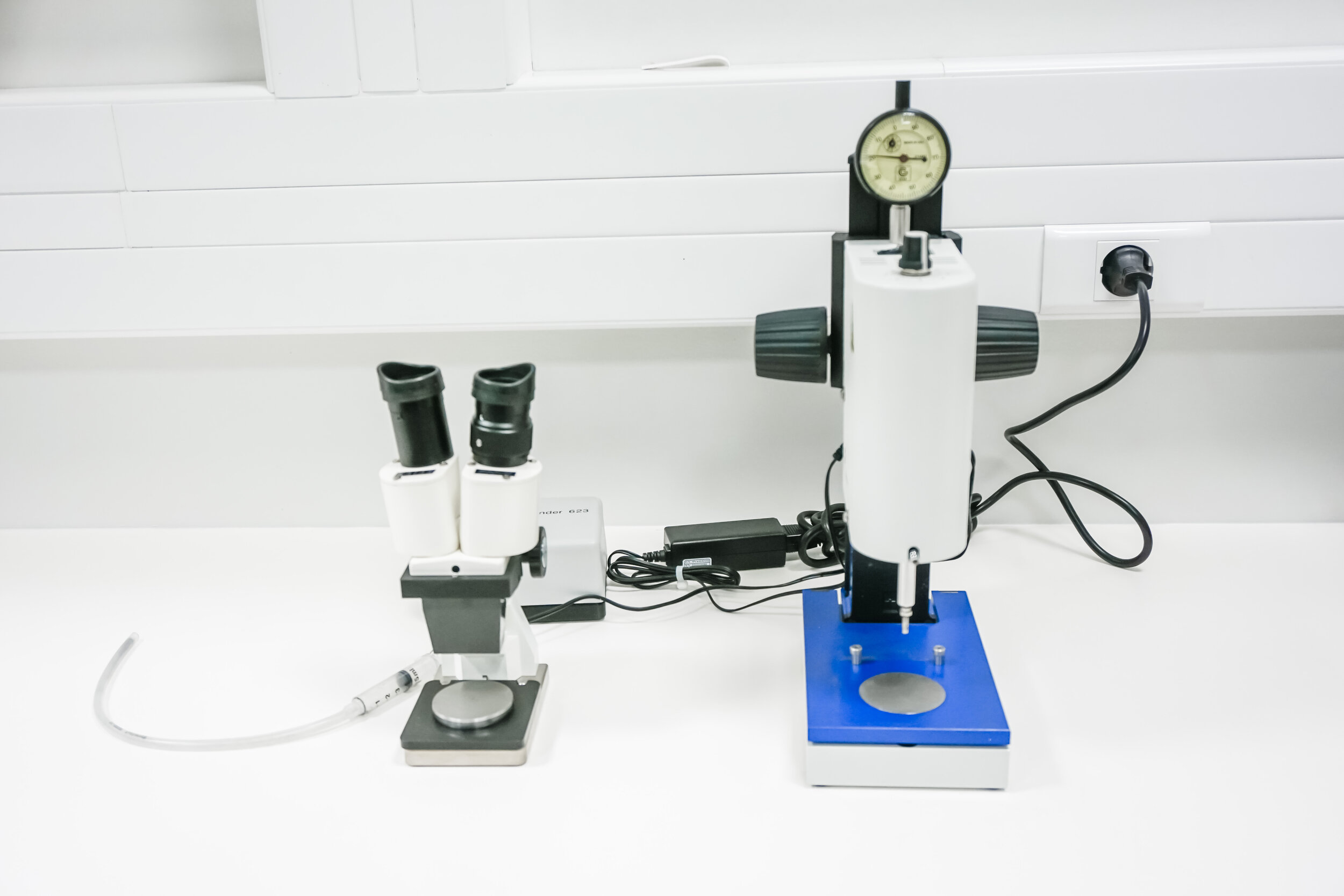
PowerTome PC Ultramicrotome RMC Boeckeler
Auto-sectioning range from <50 nm to several micrometer.
Can operate as room temperature or cryo-ultramicrotome.
PC control
Cutting speed 01.-100mm/sec
Multi-level vibration isolation system
High precision micrometer knife stage
Gatan 601 Tuned Piezo Cutting Tool –Disc Cutter
Cuts 3 mm discs out of brittle material for TEM.
Variable frequency for optimising cutting performance.
Uses high frequency vibrations with fine grain boron carbide slurry to cut material.
Gatan Precision Ion Polishing System – PIPSII
Benchtop system to produce high quality TEM-specimens with exceptionally large, clean and electron transparent regions.
Dual argon ion beam with +/- 10° tilt range.
X,Y stage that permits alignment of argon beams to region of interest on the sample.
Useable voltages as high as 8kV or as low as 100 volts for rapid thinning of bulk sample and damage free polishing of FIB lamella.
Glass Knife Maker RMC Boeckeler – GKM-2
Produces glass knifes for use with “PowerTome PC Ultramicrotome”.
“Balanced Break” Method for sharpest glass knifes
Digital readout of pressure used during glass knife making process for improved reproducibility.
Precision micrometres in order to fine adjust break position.
Nano Imprint Lithography (NIL) - Obducat EITRE® 8
Pattern replication in the micro- and nanometer range.
Excellent residual layer thickness control (sub -20 nm) across the entire imprint area, up to 200 mm substrates.
A wide variety of imprint processes such as hot embossing, thermal NIL, UV NIL and Obducat’s unique Simultaneous Thermal and UV (STU®) process
Plasma-Assisted Reative Ion Etching System – RIE (SPTS OMEGA ICP)
SPTS OMEGA ICP process module etches a wide range of materials including oxides, nitrides, polymers, low aspect ratio Si and metals.
The Omega® ICP process module uses a high density plasma source incorporating a radial coil design.
Plasma-assisted Reactive Ion Etching system – RIE (Orbotech's SPTS Technologies)
RIE -ICP system based on chlorine and fluorine chemistry
200 mm (8 inch) wafers
Etching uniformity: +/-2.5%
Selectivity Al(SiO2)/ Photoresist > 2:1
Plasma Enhanced Chemical Vapor Deposition (PECVD) system (Oxford Instruments)
Deposition of a-Si:H – intrinsic and doped; silicon dioxide (SiO2); silicon nitride (SiNx)
200 mm (8 inch) wafers
Chamber pressure < 10-7 Torr
Film uniformity < 3%
Multi-target Module for Physical Vapor Deposition – PVD (Nordiko)
DC/RF Magnetron Sputtering
200 mm (8 inch) wafers
Film uniformity ± 1% (RF Sputtering), ± 2.5% (DC Sputtering)
Roughness < 0.2nm rms for metallic films < 50nm
Heated substrate holder (up to 500 C)
Chamber base pressure: 5x10⁻⁸ Torr
Ellipsometer for in-situ optical characterization of deposited films (alpha-SE J.A. Woollam)
Spectral Range: 380 nm to 900 nm
Roating compensator technology with CCD detection
Angle of incidence: 65º, 70º, 75º or 90º
Data acquisition rate; 3 sec., 10 sec. and 30 sec.
Beam Diameter: ~3mm (collimated) and ~0.3 mm (focused)
Plasma Atomic Layer Deposition Systems (SenTech)
Based on a method of applying thin films to various substrates with atomic scale precision.
ALD is a powerful resource for advanced nanotechnology research since it allows the manufacture very precise nanometer –thick, pinhole–free and totally conformal thin films on any shape and geometry.
Moreover, ALD real time monitor is available for measuring the thickness of the ultra-thin films.


